Extra exam question E6C11
Subelement E6, CIRCUIT COMPONENTS· Group E6C
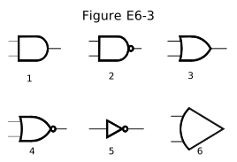
In Figure E6-3, which is the schematic symbol for the NOT operation (inversion)?
- A.2
- B.4
- C.5 (correct answer)
- D.6
WhySymbol 5 in Figure E6-3 is the schematic symbol for the NOT operation, inversion. In Figure E6-3, symbol 5 shows a simple triangle (buffer) shape with a small bubble at its output, the standard schematic symbol for an inverter, performing the NOT operation on a single input, answer C. Symbol 2 is a NAND gate, symbol 4 is a NOR gate, and symbol 6 is a plain gate shape without an inversion bubble, none of which represents the single-input NOT operation being asked for.
Published 2026-08-28 · Last updated 2026-08-28 · Question text is verbatim from the 2024-2028 NCVEC Element 4 pool (public domain); the explanation above is original writing, see our methodology.
Related questions
- E6C01What is the function of hysteresis in a comparator?
- E6C02What happens when the level of a comparator’s input signal crosses the threshold voltage?
- E6C03What is tri-state logic?
- E6C04Which of the following is an advantage of BiCMOS logic?
- E6C05Which of the following digital logic families has the lowest power consumption?