Extra exam question E7B10
Subelement E7, PRACTICAL CIRCUITS· Group E7B
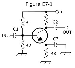
In Figure E7-1, what is the purpose of R1 and R2?
- A.Load resistors
- B.Voltage divider bias (correct answer)
- C.Self bias
- D.Feedback
WhyIn Figure E7-1, R1 and R2 provide voltage divider bias. In Figure E7-1, R1 (from the positive supply to the base) and R2 (from the base to ground) form a voltage divider that sets a stable DC voltage at the transistor's base, the standard voltage-divider bias arrangement used to establish a predictable operating point independent of the individual transistor's beta, answer B. They aren't load resistors, since the actual output load resistor is elsewhere in the circuit, and they don't function as self bias or feedback, those are separate roles filled by other components.
Published 2026-08-28 · Last updated 2026-08-28 · Question text is verbatim from the 2024-2028 NCVEC Element 4 pool (public domain); the explanation above is original writing, see our methodology.
Related questions
- E7B01For what portion of the signal cycle does each active element in a push-pull, Class AB amplifier conduct?
- E7B02What is a Class D amplifier?
- E7B03What circuit is required at the output of an RF switching amplifier?
- E7B04What is the operating point of a Class A common emitter amplifier?
- E7B05What can be done to prevent unwanted oscillations in an RF power amplifier?